Multilayer PCB: Revolutionizing Circuit Board Design
Introduction:
The demand for electronic devices with advanced function Multilayer PCB alities has led to the development of complex and high-performance printed circuit boards (PCBs). Among them, multilayer PCBs have emerged as the go-to choice for various applications due to their versatility, reliability, and compact design. This article takes an Multilayer PCB in-depth look at multilayer PCBs, exploring their manufacturing process, features, advantages, usage methods, tips on selecting the right manufacturer or factory for a Multilayer PCB production and concludes with its significance in modern electronics.
Manufacturing Process:
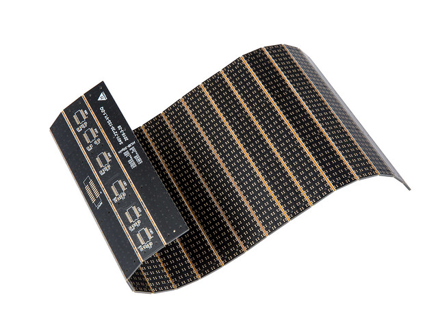
Multilayered printed circuit boards are constructed by sandwiching multiple layers of conductive copper tracks inside insulating materials such as FR-4 or polyimide films. The process involves laminating each layer onto one another using specialized adhesives. Furthermore, vias – small holes connecting different layers – play a crucial role in ensuring proper electrical connectivity Multilayer PCB across all layers.
Features:
One distinctive feature of multilayer PCBs is their ability to provide increased complexity within a compact form factor. The stacked construction allows designers to incorporate multiple signal paths while minimizing space requirements significantly. Moreover, these boards can achieve higher current-carrying capacit Ceramic PCB factory y due to wider copper traces and additional power planes dedicated solely for sufficient power distribution.
Advantages:
The use of multilayered printed circuit boards offers several advantages over traditional single-layer or double-sided ones. Fi

rstly, they enable improved heat dissipation through increased surface area availability for thermal management components like heat sinks or thermally conductive pads. Additionally, the reduced footprint enables enhanced functionality without compromising performance characteristics such as signal integrity High-density interconnect (HDI) board or impedance control.
Usage Methods:
Multilayer PCBs find extensive application across various industries including telecommunications,
automotive electronics
medical devices
aerospace
computing systems etc.
In telecommunication systems especially cellular networks require high-density interconnect (HDI) boards to support rigorous signal processing demands. The unique design possibilities offered by multilayer PCBs make them ideal for such applications.
Selecting the Right Multilayer PCB Manufacturer:
Choosing a reliable and experienced man Multilayer PCB manufacturer ufacturer is vital when opting for multilayer PCBs. A trusted manufacturer will possess in-depth knowledge of material selection, fabrication techniques, and quality control procedures necessary for ensuring product reliability. Multiple factors like industry certifications, previous custome Complex PCB r feedback, adherence to international standards should be considered while selecting an appropriate supplier or manufacturer.
Conclusion:
Multilayered printed circuit boards have become the backbone of modern electronic devices due to their exceptional performance and compact d Multilayer PCB manufacturer esign. With advancements in manufacturing techniques, these boards offer unparalleled freedom and flexibility for designers seeking complex functionalities within limited space constraints. Through careful selection of manufacturers or factories that specialize in multilayer PCB production,
one can ensure high-quality products tailored to meet specific application requirements.
Therefore, it is imperative for industries across sectors to prioritize the use of multilayer PCB technology as they continue to revolutionize t Multi-layered printed circuit board he world of electronics.