Multilayer PCB: Manufacturing, Features, Advantages and Selection Guide
Introduction:
In today’s advanced electronic world, the demand for high-performance circuit boards has significantly increased. One such te Multilayer PCB chnology that meets these demands is Multilayer PCB (Printed Circuit Board). This article explores the manufacturing process, features, advantages, usage methods, and tips on sel

ecting this exceptional product.
Manufacturing Process:
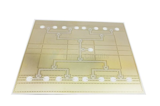
Multilayer PCBs are constructed using a complex manufacturing process. They consist of three or more laye Multilayer PCB manufacturer rs of interconnected circuits sandwiched between insulating layers. Double-sided PCBs contain only two layers of circuits while layered multilayers can have even more than twenty-four core layers! The connections between these different layers are achieved through conducting vias and plated copper pads.
Features:
One distinguishing feature of Multilayer PCBs compared to single-sided or double-sided High-density interconnect (HDI) board ones is their enhanced complexity due to multiple internal interconnections. These interconnections allow designers to integrate more functionalities into a smaller space. Additionally, High-density interconnect (HDI) boards belong to the family of multilayers but provide even greater flexibility in terms of miniaturization and component density.
Adva Multilayer PCB ntages:
The utilization of Multilayer PCBs offers several advantages over traditional options:
1. Space Efficiency: Due to their layered structure and compact design footprint, they save considerable space within the Ceramic PCB private label electronic device.
2. Enhanced Performance: The presence of internal power and signal planes minimizes the chances of electromagnetic interference (E Multilayer PCB MI), making them ideal for high-speed applications.
3. Reliability: Their sturdy construction ensures greater reliability regarding heat resistance and electrical performance stability.
4. Flexibility: With customizable layer counts as per project requirements, multilayers prov Double-sided PCB ide flexibility during circuit design.
Usage Methods:
Multilayer PCBs find extensive application across various industries including telecommunications, aerospace engineering,lthcare devices,ficiently power management systems which require precise control.r more flexible a Layered PCB pplication)
How to Select the Right Multilayer PCB?
To choose the appropriate Multilayer PCB, consider the following factors:
1. Quality: Opt for a reliable and experienced Multilayer PCB manufacturer. The use of high-quality materials and adherence to industry standards are crucial.
2. Design Compatibility: Confirm that the board layout matches your project requirements, including specific layer counts and dimensions.
3. Manufacturing Capabilities: Ensure that the selected m

anufacturer can meet your quantity and delivery time exp

ectations.
4. Certification Compliance: Depending on industry regulations, certain certifications like IPC-6012 Class 3 might be necessary to ensure product quality.
Conclusion:
Multilayer PCBs offer tremendous advantages in terms of space efficiency, enhanced performance, reliability, and flexibility for a wide range of applications. When selecting this techn Multilayer PCB manufacturer ology for your projects, it is essential to consider quality, compatibility with design specifications, manufacturing capabilities,