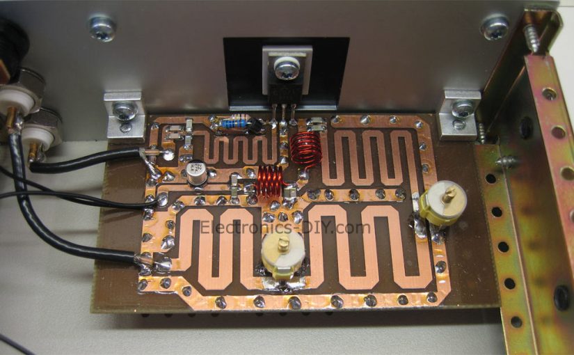
RF Amplifier PCB Design

When designing an RF amplifier PCB, there are many things to consider, such as the high-power versus low-noise ratio, as well as the output matching network and the biasing network. You’ll also want to design a PCB that’s easy to build and maintain, and it should be compatible with the rest of your electronics.
High-power vs low-noise
One of the most critical parts of the RF front end is the RF amplifier. A good RF amplifier can amplify a weak signal without boosting the noise.
There are many components to consider when designing an RF amplifier PCB. Some of the most important are input and output power, noise figure, and frequency.
For an RF amplifier PCB to operate at the right frequency, the correct gain is essential. This ensures the correct output amplitude and minimizes the risk of overloading the device.
An RF power supply is also a component to consider. A good RF power supply will have an appropriate regulator. It can be a discrete component, or a multi-stage design on a single board. The output may be routed directly to the antenna, or through a BAW or SAW filter.
An RF power supply will have a supply voltage ranging from 1.8 to 6 V. It should be designed to provide a good level of efficiency. Also, it must be able to handle the heat generated by the RF signal.
If the output is to be routed directly to the antenna, then SMD isolators may be necessary. Similarly, if the output is to go to a digital clock, then an isolator can help prevent reflections from travelling back to the RF amplifier.
A good RF amplifier PCB will have a decent noise figure. Generally, the noise figure will be less than 2 dB for small signals, and more than 2 dB for large ones.
In addition, a decent gain control strategy should be used. This will improve the monotonic SNR of the input signal as it decreases in power.
Finally, a proper transmission line design will be needed. This should take into account the dielectric dispersion of the copper.
Stages
An RF amplifier is a device which provides an amplified signal for use with radio transmitters or antennas. It can function as a power amplifier before transmission or as a low noise amplifier after transmission. The RF Amplifier PCB components used to build an RF amplifier PCB can vary, depending on the requirements of the intended application.
The basic stages of an RF amplifier are the input/splitter board, the control system and power distribution circuit, and the final stage. Each of these stages should be designed for a specific frequency, power, and gain. For example, a switch amplifier has a switch with a variable width and a pulse as the input signal.
A small signal processing circuit is located on the input signal/splitter board. This circuit is responsible for isolating the source generator and providing the appropriate noise factor for the RF amplifier. It may include a high pass or low pass filter, a variable voltage attenuator, and an equalizer.
The combined outputs of the modules in the final stage are routed to the input of the combiner. In other embodiments, the combiner may combine several signals instead of four.
The control system and power distribution circuit 102 is responsible for overall system operation. For example, it might read the status of each RF stage and then determine how to distribute the current between each RF stage.
The amplifier PCB should have the correct amount of input resistance, and should also have a suitable layout. As with any other electronic component, the wiring and circuitry should be laid out on the printed circuit board in a way that minimizes spurious emissions.
The layout of the board depends on the type of frequency, the number of layers needed, and the budget for the design. It should also take into account the packaging restrictions, if any.
Biasing network
If you’re designing a broadband RF amplifier, you might be looking for a biasing network on the PCB that reduces RF signal leakage and improves gain. This is especially true if you’re trying to build a multi-stage amplifier.
A common biasing circuit involves the use of a transmission line and chip capacitors. It may be used to bias a single-stage amplifier or a cascade amplifier. For a more robust and stable design, the circuit is supplemented with quarter-wave transformers.
In addition, an active bias controller can be used to optimize performance. Such devices can provide precise control of the input, output, and drain currents of an RF amplifier. The device can also adjust the voltage level for each individual DUT.
In a typical biasing structure for a Class A RF/microwave power amplifier, a resistive voltage divider network is employed to generate two fixed biasing voltages. These are applied to the base-emitter junctions of switching transistors.
An example of a more elaborate biasing circuit is the use of a radial stub. As shown in Figure 7, this type of circuit can be used to create a broader RF open circuit.
This method is applicable to a wide range of frequency bands. Another biasing scheme is the tri-band method, which exhibits good performance.
When designing an RF amplifier, you must consider the performance of the quiescent drain current. This affects the overall efficiency of the amplifier and the intermodulation products produced. Furthermore, it’s important to minimize the amount of power leakage.
Biasing is a complex and important part of the RF amplifier design. However, incorrect biasing can cause a sharp crossover distortion spike. Moreover, RF amplifiers are designed to perform best under specific bias conditions.
Output matching network
An output matching network for an RF amplifier PCB is designed to transfer maximum power to the RF source. This requires that the input impedance is correctly matched to the output impedance. The matching network can consist of a single shunt component, or a series capacitor and inductors.
There are a few basic steps that are needed to calculate the proper capacitance and inductance values for an RF matching circuit. Using an appropriate software program will enable the correct component values to be determined.
For example, the optimum value for an inductor may not be the same as the optimum value for an RF capacitor. To determine this, the inductance of the ground connections must be taken into consideration.
Likewise, a shunt circuit for a variable component can be optimized with RF Amplifier PCB a suitable virtual ground. A virtual ground is a surface or subsurface mounting of a capacitor. L31-L39 can be used for this purpose.
The correct combination of components will also protect the circuit from high voltage stress. An overvoltage conditioning circuit 182 is one way to do this. It can switch off all active switches in the event of an overvoltage.
Choosing the right type of capacitance will allow the power to be transferred to the RF source. Choosing the wrong type will cause excessive noise and distortion. Similarly, selecting the wrong type of inductor will affect the input impedance.
Using a gain amplifier, signal quality can be improved. This is especially true for a shallow signal from an antenna. In addition, a gain amplifier eliminates extra noise.
If a low input impedance is required, a buffer design will do the trick. This type of circuit consists of a series inductor that cancels the reactive parts of the matching network. Another shunt component, a variable capacitor, provides the correct second shunt capacitance value.
RF amplifier PCB design challenges
Achieving an efficient RF amplifier PCB design is not always easy. The layout, power, and materials that are used must be carefully considered. There are also environmental requirements that must be taken into account.
Often, RF PCBs are made from multiple layers. These layers can be manufactured with different materials. However, these must all meet performance and thermal requirements. In addition, they should be scaled correctly. This will affect the overall performance of the product.
Common materials for RF PCBs include polycarbonate, ceramics, and hydrocarbons. Other options are Teflon and exotic ceramics.
The first step in designing an RF PCB is to understand the characteristics of the material that will be used. A material’s dielectric constant, or eR, can impact the performance of the board.
The dielectric constant can be found using online tools. If the PCB is to be used in an extreme environment, such as underwater, special characteristics will need to be considered.
One way to minimize crosstalk is to make traces connecting RF components as short as possible. Alternatively, via holes can be added to reduce parasitic inductance.
Lastly, it is important to avoid discontinuous ground planes. Ground planes should be near or adjacent to the high-frequency components. Otherwise, they will disrupt the operation of the amplifier.
Another challenge in designing an RF PCB is the size. For a small PCB, it may be easier to use a single layer. But this can create problems when the density of the board increases.
Besides being a significant challenge, inductance can also play a role. Ideally, inductance should be kept as low as possible. It can be reduced by providing sufficient ground connections to each RF component.